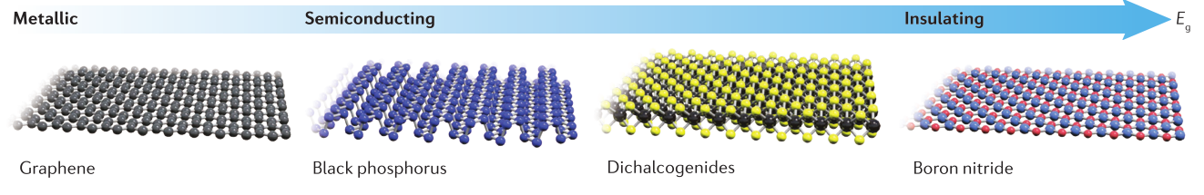
MOTIVATION Since the invention of the first germanium transistor by Bardeen, Brattain and Shockley in 1947 , the semiconductor industry has striven for progress in on-chip circuit technologies that underpin our daily lives today. The modern age of electronics is rapidly approaching a paradigm shift, as Moore’s law begins to falter beyond the 10-nm node regime . The International Roadmap for Semiconductor Technology (ITRS) has recently been replaced by the IDRS, reflecting the change in focus with regard to new integrated circuit (IC) design and implementations of nanotechnology in everyday devices. As the Internet of Things (IoT) and neural network computing come to the fore of scientific research worldwide, efforts have shifted to multidisciplinary approaches combining various areas of physics, chemistry, engineering and biology. Spearheading this movement in the field of nanoscience is the area of two-dimensional (2D) materials, where recently-discovered allotropes of well-known chemical compounds have proven to exhibit extraordinary properties when studied on the nanoscale. Graphene, the prototypical 2D material, has attracted tremendous interest since its discovery in 2004 . Owing to its superlative physical properties such as high carrier mobility , minimum electrical conductivity , mechanical strength and thermal conductivity , it has garnered much institutional funding and scrutiny from both experts and the public. In recent years, doubts have been cast as to the fruition of graphene-related research when it comes to everyday applications. Long-heralded as the successor to silicon-based technology, planar carbon faces considerable challenges before it can become ubiquitous in high-frequency switching devices and flexible electronic displays , . Researchers have thus moved beyond graphene in search of low-dimensional materials that could prove useful in new generation flexible electronics, photodetectors, LEDs and tunneling transistors. The family of transition metal dichalcogenides (TMDs) is populated by compounds whose unique functionalities and versatility of physical properties offers complementary properties to that of graphene and existing silicon-based fabrication processes. The ability to manipulate these properties on the nanoscale is a central theme of this thesis, with particular focus on electronic properties and devices which could be fabricated using TMDs.